Key Elements of Effective Semiconductor Cleanroom Designs Across Applications
Modern electronics depend on semiconductor cleanrooms to ensure chips are manufactured without contamination or defects. These environments are critical to maintaining performance and precision as industries push for smaller, faster, and more reliable components.
In this article, we’ll explain what semiconductor cleanrooms are, where they’re used, and what key elements make them effective for high-precision chip manufacturing.
What Are Semiconductor Cleanrooms?
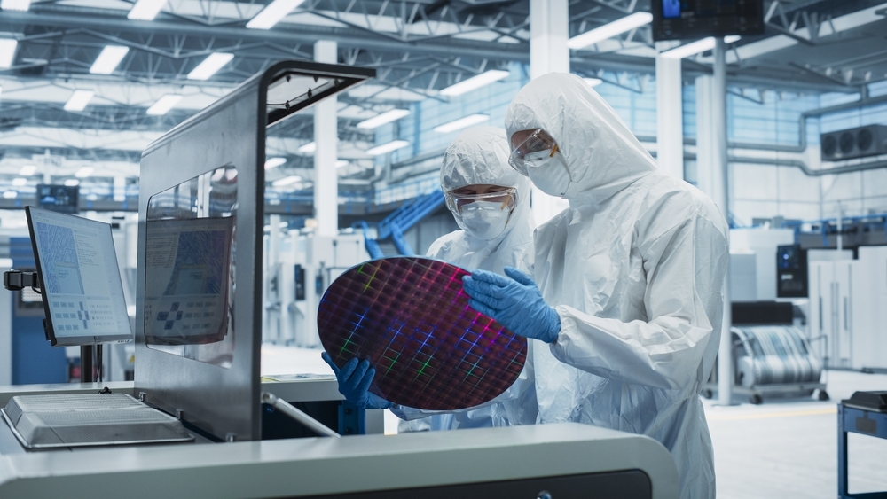
A semiconductor cleanroom is a specially constructed, highly filtered environment designed to limit airborne particulates, temperature fluctuations, humidity, and static — all of which can interfere with microelectronics fabrication. Nanoscale processes like photolithography, doping, and etching are extremely vulnerable to external variables. Even a human hair, at about 75,000 nanometers wide, is a massive threat in this context.
Semiconductor cleanrooms are classified by the ISO 14644-1 standard (among others), which defines cleanliness based on the number of particles per cubic meter. They typically require:
- ISO Class 4–6, allowing just 10 to 1,000 particles (≥0.1 µm) per cubic meter
- Stringent environmental controls (temperature, humidity, airflow)
- Specialized materials and processes to prevent outgassing, static discharge, and contamination
Industries That Rely on Semiconductor Cleanrooms
Semiconductor cleanrooms are critical across a number of industries, including:
|
Industry |
Application |
Notes |
|
Computing |
CPUs, GPUs, memory, data storage |
Requires extremely tight tolerances |
|
Advanced driver assistance systems (ADAS) sensors, electric vehicle chips, power systems |
Often requires ASTM (American Society for Testing and Materials) compliance for reliability |
|
|
Navigation, communication, and control systems |
Must meet NASA and mil-spec cleanliness levels |
|
|
Robotics |
Microcontrollers, precision feedback systems |
Sensitive to particle and static interference |
|
Appliances |
Smart sensors, control chips |
Cleanroom ensures cost-effective mass production |
|
Lab-on-chip, diagnostic microdevices |
Overlaps with pharmaceutical and medical device cleanroom regulations |
Semiconductor Cleanroom Design Standards and Compliance
While ISO classifications define the basic cleanliness of the room, semiconductor cleanrooms often need to comply with additional application-specific standards like:
- ASTM F24, F51, and F2322 for automotive-grade components
- NASA-STD-8739 and MIL-STD-883 for aerospace environments
- GMP regulations for biotech and diagnostic chip manufacturing
These standards influence everything from material selection to testing procedures and must be factored into the cleanroom’s design from day one.
5 Semiconductor Cleanroom Design Considerations
1. Advanced HVAC and Filtration Systems
To maintain airborne contaminant control, semiconductor cleanrooms rely on HEPA or ULPA filtration systems integrated into precision HVAC setups. These systems deliver laminar airflow to prevent cross-contamination, maintain positive pressure to prevent unfiltered air infiltration, and ensure tight temperature and humidity control (often ±1°F and ±1% RH).
Learn more about cleanroom HVAC design >>
2. Material Selection and Outgassing Control
Semiconductor cleanrooms must use low-outgassing materials like stainless steel, anodized aluminum, and select polymers to prevent the release of harmful chemical vapors. All materials should be chemically inert under operational conditions, non-particulating and easy to clean, and compatible with cleaning agents and sterilization methods.
Tools like the NASA Outgassing Database can help you identify approved materials.
3. Static Control & Electrostatic Discharge (ESD) Protection
Semiconductors are highly susceptible to electrostatic discharge. As a result, semiconductor cleanrooms must integrate:
- Static-dissipative flooring, work surfaces, and garments
- Grounding wrist straps and mats
- ESD-safe packaging and tools
All personnel and equipment must be grounded, and entry procedures should ensure charge neutrality.
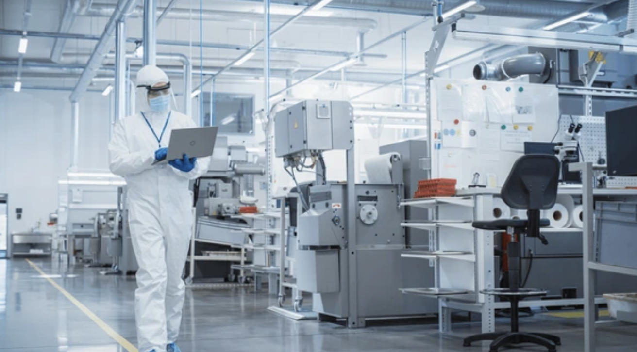
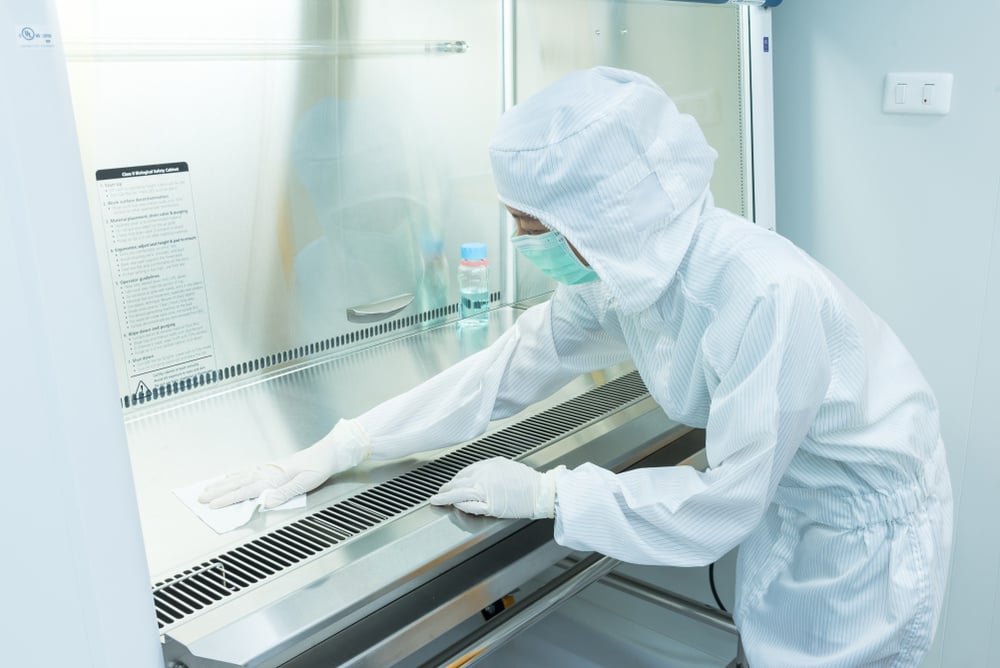
4. Operator Training and Protocols
People are the largest source of contamination in cleanrooms. That’s why comprehensive training is a critical part of every semiconductor cleanroom program. Training covers:
- Proper gowning and donning procedures
- Movement restrictions to prevent particle generation
- Tool and material handling protocols
- Routine cleaning and emergency procedures
Strict standard operating processes (SOPs) and ongoing retraining help enforce compliance and cleanliness.
5. Humidity and Temperature Control
Semiconductor processes often require tight temperature tolerances (±1°F) to ensure chemical process consistency and controlled humidity (~30–50%) to prevent static buildup and moisture absorption.
Dedicated environmental control systems, redundant sensors, and real-time monitoring help ensure stability and minimize costly downtime.
Build Smarter, Safer Semiconductor Facilities with Encompass
Effective semiconductor cleanroom design is a specialized discipline that demands a deep understanding of regulatory compliance, process integration, and material science. At Encompass, we specialize in turnkey cleanroom solutions tailored to the unique challenges of semiconductor manufacturing. From early-stage planning to final commissioning, our team brings precision, compliance, and proven results to every project.
Get in touch with us today to discuss your semiconductor cleanroom build.