bg-img

Semiconductor cleanrooms engineered for precision

Contamination control is everything in semiconductor fabrication. At Encompass Cleanrooms, we design ISO-classified environments that support ultra-clean production, high yields, and cutting-edge innovation.

bg-img

Defend delicate processes from contamination

Semiconductors are the backbone of modern technology, powering everything from smartphones and medical devices to electric vehicles and defense systems. As demand for faster, smaller, and more powerful electronics grows, reliable semiconductor production is more critical than ever.

Cleanrooms are essential to maintaining yield, improving process reliability, and meeting the strict demands of this industry. Encompass Cleanrooms specializes in ISO Class 4–8 cleanrooms tailored to each stage of the semiconductor lifecycle. 


Supporting sensitive semiconductor applications

As semiconductor components shrink in size and increase in complexity, even microscopic particles can compromise functionality or ruin entire production batches. From wafer fabrication to final packaging, we deliver contamination control solutions that align with your exact process requirements.

Wafer fabrication

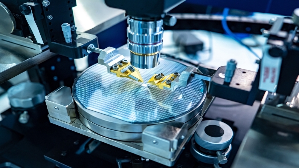
Ultra-clean environments are critical during lithography, etching, and deposition processes to prevent defects that can render entire wafers unusable.

Microchip assembly & packaging

Cleanrooms help maintain the integrity of die bonding, wire bonding, and encapsulation, ensuring reliable chip performance in final applications.

Testing & inspection

Particles and static electricity can skew test results or damage sensitive components. Cleanrooms provide the stability needed for accurate QA and device reliability.

bg-img

Ideal cleanroom types for semiconductor facilities

Semiconductor manufacturing facilities require highly controlled cleanrooms that support continuous operation, precise airflow, and adaptable layouts. We recommend hardwall and rigidwall cleanrooms, based on your ISO classification and production goals.

Hardwall cleanrooms:

Built for the most stringent ISO Class compliance, hardwall cleanrooms maintain constant airflow and pressurization. Ideal for critical processes like photolithography or chemical vapor deposition (CVD).

Rigidwall cleanrooms:

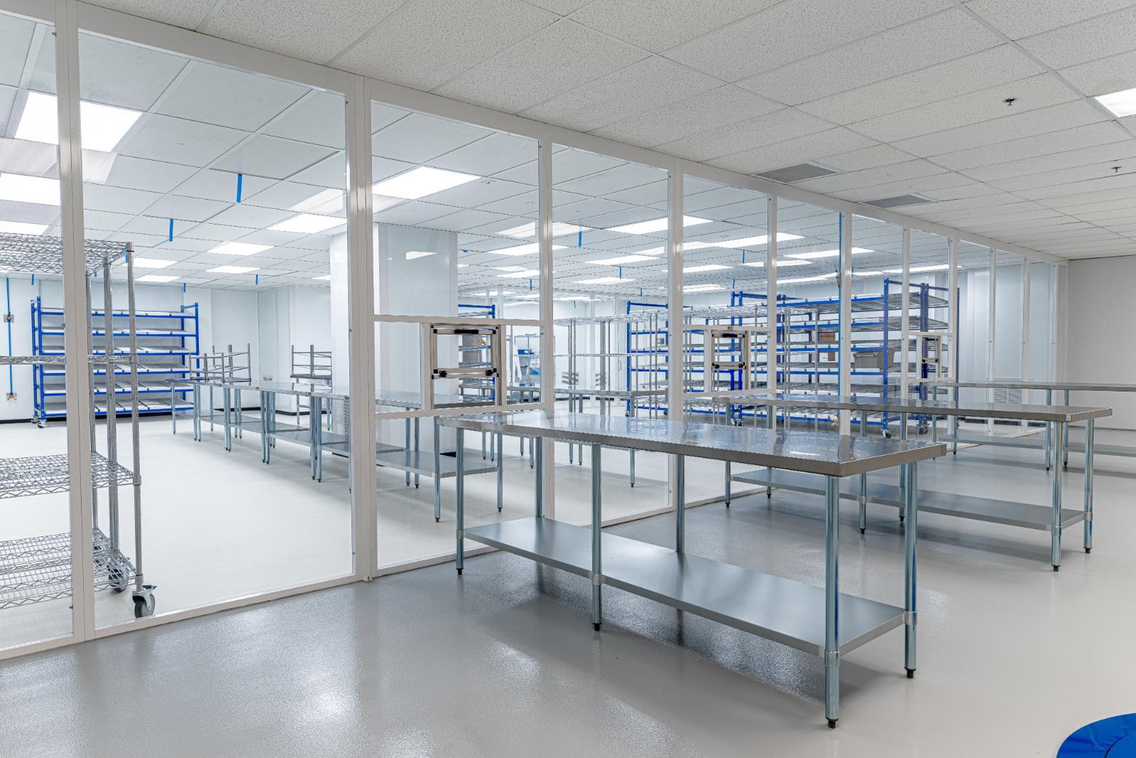
A cost-effective and flexible solution for ISO Class 5-8 environments. Their clear Rigidpanels support assembly, testing, and packaging applications while providing excellent visibility and control.

Industry expertise for every semiconductor process

Our cleanroom specialists understand the demands of semiconductor fabrication. Whether you're building a new space or upgrading an existing one, we design with performance, compliance, and uptime in mind.

keystone-med-pack-web-web-6

Designed for precision, backed by service

Semiconductor cleanrooms must maintain performance 24/7. That’s why Encompass offers proactive maintenance services like airflow validation, filter replacement, environmental monitoring, and ESD control to keep your facility operating at peak performance.

Our service plans help ensure you maintain ISO compliance and production efficiency, day in and day out.

What ISO classifications are required for different stages of semiconductor manufacturing?

Semiconductor manufacturing spans a wider classification range than almost any other industry, from ISO Class 4 in the most critical photolithography and deposition processes to ISO Class 7–8 for packaging, testing, and inspection.

  • Wafer fabrication (lithography, etching, chemical vapor deposition) typically requires the tightest classifications.
  • Die bonding, wire bonding, and encapsulation are generally less stringent, operating in the ISO Class 5–7 range.
  • Final testing and inspection can often be performed in ISO Class 7–8 environments.

The classification at each stage is determined by the minimum particle size that can cause a defect in the process. And as feature sizes on modern chips have shrunk into the nanometer range, the particle counts that constitute a contamination event have become increasingly smaller and numerous.

How does contamination at the sub-micron level affect semiconductor yield, and what does that mean for cleanroom design?

A single particle smaller than the human eye can detect is large enough to render a semiconductor die unusable. Feature sizes in current processes are measured in nanometers (for context, a human hair is roughly 70,000 nanometers wide), and contamination at that scale causes defects that are basically invisible until electrical testing reveals them as failures.

Yield implications are direct and financially significant, since contamination that ruins a portion of a wafer means lost revenue on every die that doesn't pass. That means cleanroom design for semiconductor fabrication is as much about eliminating contamination pathways as it is about achieving a classification number.

Attention to airflow uniformity, material transfer protocols, equipment outgassing, personnel movement patterns, and surface finish is critical. Basically, every variable that contributes to particle generation or transport inside the controlled space must be considered.

What HVAC and airflow requirements are unique to semiconductor cleanrooms?

Semiconductor cleanrooms, and particularly for wafer fabs operating at ISO Class 4–5, require unidirectional (laminar) airflow configurations that push air vertically from ceiling to floor at consistent velocity across the entire work area. This is fundamentally different from the turbulent dilution airflow used in less stringent environments.

Achieving laminar flow at the required classifications demands very high air change rates, high HEPA or ULPA filtration ceiling coverage, and precisely balanced HVAC systems that can maintain consistent pressure, temperature, and humidity across large footprints. Temperature and humidity stability also matter in semiconductor manufacturing beyond contamination control. For example, thermal variation affects the dimensional stability of wafers and precision equipment during processing.

Designing these systems correctly from the start requires detailed engineering of airflow, filtration, and mechanical systems before any construction begins.

How do electrostatic discharge controls factor into semiconductor cleanroom design?

Electrostatic discharge (ESD) is a parallel contamination risk to particulates in semiconductor manufacturing (and a more immediately destructive one in some processes). And ESD events can damage or destroy semiconductor devices at charge levels far below what a human can feel, making personnel, equipment, and surfaces all potential sources of risk.

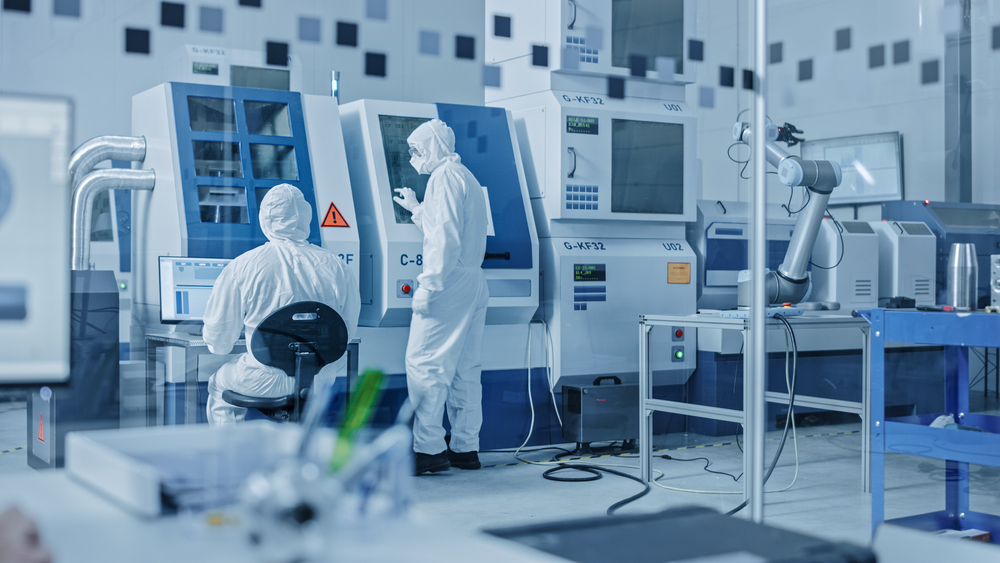
Cleanroom design for semiconductor applications addresses ESD through a combination of static-dissipative flooring and surfaces, grounding systems for equipment and personnel, ionization systems that neutralize static charge in critical work areas, and gowning protocols that include ESD-rated garments and footwear.

These controls need to be integrated into the cleanroom. The materials, surfaces, and mechanical systems specified during design determine how effectively ESD risk can be managed in operation.

Can a semiconductor cleanroom be designed to accommodate multiple process nodes or future technology generations?

Yes, to a degree. But the final answer depends heavily on what's driving the change. If future process requirements involve stricter ISO classifications, additional filtration capacity, or different airflow configurations, the cleanroom will likely need substantial modification rather than simple reconfiguration. Those kinds of changes are tied to the HVAC and filtration systems, which are less flexible than the structural elements.

Where modular construction provides real adaptability is in layout and footprint, since equipment configurations can change, zones reconfigured, and the physical structure expanded or reorganized more readily than a stick-built facility allows.

For semiconductor manufacturers planning a facility that will need to evolve with technology roadmaps, designing with future flexibility in mind, including adequate infrastructure capacity for more demanding process requirements, is worth building into the initial project scope rather than retrofitting later.

Trusted experts in semiconductor cleanroom design

Trust Encompass for semiconductor cleanrooms engineered with technical precision and built for long-term yield and reliability in high-tech manufacturing.